- 您现在的位置:买卖IC网 > Sheet目录1998 > ICS87946AYILFT (IDT, Integrated Device Technology Inc)IC CLOCK GENERATOR 32-LQFP
ICS87946AYI REVISION B JUNE 22, 2012
3
2012 Integrated Device Technology, Inc.
ICS87946I Data Sheet
LOW SKEW, ÷1, ÷2 LVCMOS/LVTTL CLOCK GENERATOR
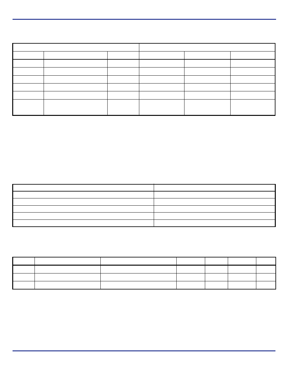
Table 3. Function Table
Absolute Maximum Ratings
NOTE: Stresses beyond those listed under Absolute Maximum Ratings may cause permanent damage to the device.
These ratings are stress specifications only. Functional operation of product at these conditions or any conditions beyond
those listed in the DC Characteristics or AC Characteristics is not implied. Exposure to absolute maximum rating conditions for
extended periods may affect product reliability.
DC Electrical Characteristics
Table 4A. Power Supply DC Characteristics, VDD = VDDX = 3.3V ± 0.3V, TA = -40°C to 85°C
NOTE 1: VDDX denotes VDDA, VDDB, VDDC.
Inputs
Outputs
MR/nOE
DIV_SELA
DIV_SELB
DIV_SELC
QA0:QA2
QB0:QB2
QC0:QC3
1
X
High-Impedance
00
X
fIN/1
Active
01
X
fIN/2
Active
0X
0
X
Active
fIN/1
Active
0X
1
X
Active
fIN/2
Active
0
X
0
Active
fIN/1
0
X
1
Active
fIN/2
Item
Rating
Supply Voltage, VDD
4.6V
Inputs, VDD
-0.5V to VDD + 0.5V
Outputs, VDD
-0.5V to VDDX+ 0.5V
Package Thermal Impedance,
θ
JA
47.9
°C/W (0 lfpm)
Storage Temperature, TSTG
-65
°C to 150°C
Symbol
Parameter
Test Conditions
Minimum
Typical
Maximum
Units
VDD
Positive Supply Voltage
3.0
3.3
3.6
V
VDDX
Output Supply Voltage; NOTE 1
3.0
3.3
3.6
V
IDD
Power Supply Current
85
mA
发布紧急采购,3分钟左右您将得到回复。
相关PDF资料
ICS87949AYILFT
IC CLOCK GEN LVCMOS 52-LQFP
ICS87950BYILF
IC CLK MULT LVCMOS/LVTTL 32-LQFP
ICS87952AYI-147LF
IC CLK MULT/ZD BUFFER 32-LQFP
ICS87972DYI-147LF
IC CLK MULT/ZD BUFFER 52-LQFP
ICS87973DYI-147LF
IC CLK MULT/ZD BUFFER 52TQFP
ICS87973DYILFT
IC CLK MULT/ZD BUFFER 52-LQFP
ICS87974CYILF
IC CLK GEN LVCMOS/LVTTL 52-LQFP
ICS894D115AGI-04LF
IC CLK/DATA RECOVERY 20-TSSOP
相关代理商/技术参数
ICS87949AYI
制造商:ICS 功能描述:
ICS87949AYILF
功能描述:IC CLK GENERATOR /1 /2 52-LQFP RoHS:是 类别:集成电路 (IC) >> 时钟/计时 - 时钟发生器,PLL,频率合成器 系列:HiPerClockS™ 标准包装:2,000 系列:- 类型:PLL 频率合成器 PLL:是 输入:晶体 输出:时钟 电路数:1 比率 - 输入:输出:1:1 差分 - 输入:输出:无/无 频率 - 最大:1GHz 除法器/乘法器:是/无 电源电压:4.5 V ~ 5.5 V 工作温度:-20°C ~ 85°C 安装类型:表面贴装 封装/外壳:16-LSSOP(0.175",4.40mm 宽) 供应商设备封装:16-SSOP 包装:带卷 (TR) 其它名称:NJW1504V-TE1-NDNJW1504V-TE1TR
ICS87949AYILFT
功能描述:IC CLOCK GEN LVCMOS 52-LQFP RoHS:是 类别:集成电路 (IC) >> 时钟/计时 - 时钟发生器,PLL,频率合成器 系列:HiPerClockS™ 标准包装:1,000 系列:- 类型:时钟/频率合成器,扇出分配 PLL:- 输入:- 输出:- 电路数:- 比率 - 输入:输出:- 差分 - 输入:输出:- 频率 - 最大:- 除法器/乘法器:- 电源电压:- 工作温度:- 安装类型:表面贴装 封装/外壳:56-VFQFN 裸露焊盘 供应商设备封装:56-VFQFP-EP(8x8) 包装:带卷 (TR) 其它名称:844S012AKI-01LFT
ICS87950BYILF
功能描述:IC CLK MULT LVCMOS/LVTTL 32-LQFP RoHS:是 类别:集成电路 (IC) >> 时钟/计时 - 时钟发生器,PLL,频率合成器 系列:HiPerClockS™ 标准包装:1,000 系列:- 类型:时钟/频率合成器,扇出分配 PLL:- 输入:- 输出:- 电路数:- 比率 - 输入:输出:- 差分 - 输入:输出:- 频率 - 最大:- 除法器/乘法器:- 电源电压:- 工作温度:- 安装类型:表面贴装 封装/外壳:56-VFQFN 裸露焊盘 供应商设备封装:56-VFQFP-EP(8x8) 包装:带卷 (TR) 其它名称:844S012AKI-01LFT
ICS87950BYILFT
功能描述:IC CLOCK MULT 1-9 32-LQFP RoHS:是 类别:集成电路 (IC) >> 时钟/计时 - 时钟发生器,PLL,频率合成器 系列:HiPerClockS™ 标准包装:1,000 系列:- 类型:时钟/频率合成器,扇出分配 PLL:- 输入:- 输出:- 电路数:- 比率 - 输入:输出:- 差分 - 输入:输出:- 频率 - 最大:- 除法器/乘法器:- 电源电压:- 工作温度:- 安装类型:表面贴装 封装/外壳:56-VFQFN 裸露焊盘 供应商设备封装:56-VFQFP-EP(8x8) 包装:带卷 (TR) 其它名称:844S012AKI-01LFT
ICS87951AYI-147LF
功能描述:IC BUFFER ZD 1-9 LOW SKEW 32LQFP RoHS:是 类别:集成电路 (IC) >> 时钟/计时 - 时钟发生器,PLL,频率合成器 系列:HiPerClockS™ 标准包装:1,000 系列:- 类型:时钟/频率合成器,扇出分配 PLL:- 输入:- 输出:- 电路数:- 比率 - 输入:输出:- 差分 - 输入:输出:- 频率 - 最大:- 除法器/乘法器:- 电源电压:- 工作温度:- 安装类型:表面贴装 封装/外壳:56-VFQFN 裸露焊盘 供应商设备封装:56-VFQFP-EP(8x8) 包装:带卷 (TR) 其它名称:844S012AKI-01LFT
ICS87951AYI-147LFT
功能描述:IC BUFFER ZD 1-9 LOW SKEW 32LQFP RoHS:是 类别:集成电路 (IC) >> 时钟/计时 - 时钟发生器,PLL,频率合成器 系列:HiPerClockS™ 标准包装:1,000 系列:- 类型:时钟/频率合成器,扇出分配 PLL:- 输入:- 输出:- 电路数:- 比率 - 输入:输出:- 差分 - 输入:输出:- 频率 - 最大:- 除法器/乘法器:- 电源电压:- 工作温度:- 安装类型:表面贴装 封装/外壳:56-VFQFN 裸露焊盘 供应商设备封装:56-VFQFP-EP(8x8) 包装:带卷 (TR) 其它名称:844S012AKI-01LFT
ICS87951AYILF
功能描述:IC CLK ZDB 1:9 180MHZ 32LQFP RoHS:是 类别:集成电路 (IC) >> 时钟/计时 - 时钟发生器,PLL,频率合成器 系列:HiPerClockS™ 标准包装:2,000 系列:- 类型:PLL 频率合成器 PLL:是 输入:晶体 输出:时钟 电路数:1 比率 - 输入:输出:1:1 差分 - 输入:输出:无/无 频率 - 最大:1GHz 除法器/乘法器:是/无 电源电压:4.5 V ~ 5.5 V 工作温度:-20°C ~ 85°C 安装类型:表面贴装 封装/外壳:16-LSSOP(0.175",4.40mm 宽) 供应商设备封装:16-SSOP 包装:带卷 (TR) 其它名称:NJW1504V-TE1-NDNJW1504V-TE1TR